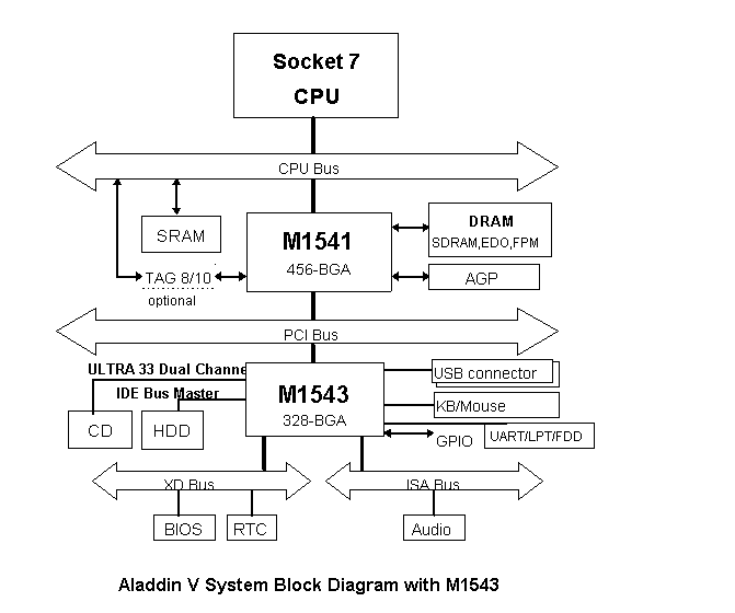
INTRODUCTION
Aladdin-V is the fifth generation
586 chipset from AcerLabs. It maintains the
best system architecture
(2-chip solution) to achieve the best system
performance with the lowest
system cost (TTL-free). Aladdin-V consists of
two BGA chips to give the
586-class system a complete solution with most
up-to-date features and
architecture for the most engaging multimedia/ multi-
threading OS and software
applications. It utilizes the modern BGA package
to improve the AC characterization
, resolves system bottleneck and make
the system manufacturing
easier.
M1541 includes the higher
CPU bus frequency (up to 100 MHz) interface for
all socket 7 compatible
processors, PBSRAM and Memory Cache L2 control-
ler, internal MESI tag
bits (16K*2) and Tag RAM (16K*10) to reduce cost
and enhance performance,
high performance FPM/EDO/SDRAM DRAM
controller, PCI 2.1 compliant
bus interface, smart deep buffer design for CPU
-to-DRAM, CPU-to-PCI, and
PCI-to-DRAM to achieve the best system
performance, and also the
highly efficient PCI fair arbiter. M1541 also provides
the most flexible 64-bit
memory bus interface for the best DRAM upgrade-
ability and ECC/Parity design
to enhance the system reliability.
With the AGP interface design,
the dedicated PCI_66 AGP interface can be
concurrent with CPU and
PCI interface. The deep buffer of the read and write
buffer design makes the
utilization of memory bandwidth more efficient. The
interface supports AGP specification
V1.0. Supports up to 128 entries table
look aside buffer for Graphic
Address Remapping Table (GART). The inter-
face not only supports the
AGP 66MHz PCI protocol, but also the AGP 1X
and 2X sideband
address function.
With the concurrent bus design,
PCI-to-PCI access can run concurrently
with CPU-to-L2 and CPU-to-DRAM
access, PCI-to-DRAM access can run
concurrently with CPU-to-L2
access. M1541 also supports the snoop ahead
feature to achieve the PCI
master full bandwidth access (133Mbytes). M1541
also provides the enhanced
power management features including ACPI
support, suspend DRAM refresh,
and internal chip power control to support
Microsoft On
Now technology OS.
M1543 provides the best desktop
system solution. M1543 integrates ACPI
support, green function,
2-channel dedicated Ultra-33 IDE Master controller
, 2-port USB controller,
SMBus controller, PS/2 Keyboard/Mouse controller
and the Super I/O (Floppy
Disk Controller, 2 serial port/1 parallel port) support.
The built-in I/O in M1543
is an advanced Super I/O controller solution to the
basic IBM PC, XT, AT and
notebook peripherals. It incorporates two full
function universal asynchronous
receiver/ transmitters (UARTs), a flexible
high performance internal
data separator with send/receive 16 byte FIFOs. It
is suitable for notebook
computers since it has Serial Infra Red for wireless
communications with other
devices. It can swap your drives A & B. It features
basic functions such as
standard mode, enhanced mode, high speed mode.
It supports SPP, PS/2, EPP
and ECP parallel port. It also has a programmable
baud rate generator. It
has high performance power management for FDC,
UART and parallel port.
Furthermore, Aladdin V is
designed to meet the requirements of all socket 7
process-ors including business,
multimedia and high performance CPU file
servers.
M1541 (AGP, CPU-to-PCI Bridge, Memory Cache & Buffer Controller)
Supports all socket 7 processors.
- Supports linear wrap mode for Cyrix M1 & M2
- Supports Write Allocation feature for AMD K6Supports Pipelined-Burst SRAM/Memory Cache- Supports Pseudo Synchronous PCI bus access
(CPU bus 75MHz - PCI bus 30Mhz,
CPU bus 83.3MHz - PCI bus 33Mhz,
CPU bus 100MHz - PCI bus 33Mhz)
- Direct mapped, 256KB/512KB/1MBSupports FPM/EDO/SDRAM DRAMs- Write-Back/Dynamic-Write-Back cache policy
- Built-in 16K*2 bit SRAM for MESI protocol to reduce cost and
enhance performance- Built-in 16K*10 bit SRAM for TAG data to reduce cost and
enhance performance- External Tag RAM free for L2 less than or equal to 512KB
- Cacheable memory up to 512MB with 10-bit Tag SRAM when
using 512KB L2 cache, 1GB when using 256KB L2 cache- 3-1-1-1-1-1-1-1 for Pipelined Burst SRAM/ Memory Cache at back
-to-back burst read and write cycles.- Supports 3.3V/5V SRAMs for Tag Address.
- Supports CPU Single Read Cycle L2 Allocation.
- 8 RAS Lines up to 1GByte support
- 64-bit data path to MemorySynchronous/Pseudo Synchronous 25/30/33MHz 3.3V/5V tolerance PCI interface- Symmetrical/Asymmetrical DRAMs
- 3.3V or 5V DRAMs
- No buffer needed for RASJ and CASJ and MA
- CBR and RAS-only refresh for FPM
- CBR and RAS-only refresh and Extended refresh and self refresh
for EDO- CBR and Self refresh for SDRAM
- 32 QWORD deep merging buffer for 3-1-1-1-1-1-1-1 posted write
cycle to enhance high speed CPU burst access- 6-3-3-3-3-3-3-3 for back-to-back FPM read page hit
5-2-2-2-2-2-2-2 for back-to-back EDO read page hit
6-1-1-1-2-1-1-1 for back-to-back SDRAM read page hit
x-2-2-2 for retired data for posted write on FPM and EDO page-hit
x-1-1-1 for retired data for posted write SDRAM page-hit
- Enhanced DRAM page miss performance
- Supports 64Mbit (16M*4, 8M*8, 4M*16) technology of DRAMs
- Supports programmable-strength RAS/CAS/ MWEJ/MA buffers.
- Supports Error Checking & Correction (ECC) and Parity for DRAM
- Supports 4 single-sided DIMMs based on x4 DRAMs
- Supports 4 single and double-sided DIMMs based on x8 and x16
DRAMs
- Concurrent PCI architectureEnhanced Power Management- PCI bus arbiter: Five PCI masters and M1533/ M1543/M1553 (ISA
Bridge) and AGP Master supported- 6 DWORDs for CPU-to-PCI Memory write posted buffers
- Converts back-to-back CPU to PCI memory write to PCI burst cycle
- 48/22 DWORDs for PCI-to-DRAM Write-posted/ Read-
prefetching buffers- PCI-to-DRAM up to 133 MB/sec bandwidth (even when L1/L2
write back)- L1/L2 pipelined snoop ahead for PCI-to-DRAM cycle
- Supports PCI mechanism #1 only
- PCI spec. 2.1 support. (N(32/16/8)+8 rule, passive release, fair
arbitration)- Enhanced performance for Memory-Read-Line and Memory-Read
-Multiple and Memory-write- Invalidate PCI commands.
- ACPI supportAccelerated Graphics Port (AGP) Interface- Supports PCI bus CLKRUN function
- Supports Dynamic Clock Stop
- Supports Power On Suspend
- Supports Suspend to Disk
- Supports Suspend to DRAM
- Self Refresh during Suspend
- Supports AGP specification V1.035x35 mm 456-pin BGA package- Supports up to 128 entries table look aside
buffer for Graphic Address Remapping Table
(GART)
- AGP 66MHz PCI protocol
- AGP 1X and 2X sideband address function
- 32 entries Request queue
- 32 QWORDs Read buffer
- 16 QWORDs Write buffer
M1543 (PCI-to-ISA Bus Bridge with Super I/O)
PCI interface
PMU features
- ON- Standby
- Sleep (Power on Suspend)
- Suspend (Suspend to DRAM)
- Suspend to Disk
- Soft-Off
- Mechanical Off
- Video- Audio
- Harddisk
- Floppy
- Serial Ports
- Parallel Port
- Keyboard
- 6 programmable I/O groups
- 3 programmable memory spaces
- AC Power- Docking insert
- Eject
- Power Button- Modem Ring
- RTC alarm
- Modem Ring- RTC alarm
- Docking insert
- Power Button
- USB events
- IRQ
- Serial IRQ
- General Purpose Input event
- CPUCLK stop control- PCICLK stop control
- PLL stop control
- Slowdown Frequency control
- Software compatible with 82077 and supports 16-byte data FIFOs- High performance internal data separator
- Supports standard 1 Mbps / 500 Kbps / 300 Kbps / 250 Kbps
data rate- Supports 3 modes of 3.5" FDD (720K/ 1.44MB/2.88MB)
- Swappable drives A and B
- Standard mode- IBM PC/XT, PC/AT and PS/2 compatible Bi-directional parallel
port- Enhanced mode
- Enhanced Parallel Port (EPP) compatible
- High speed mode
- Microsoft and Hewlett Packard Extended Capabilities Port (ECP)
compatible- includes protection circuit against damage caused when printer
is powered up, or operated at higher voltages
- Two high performance 16550 compatible UARTs with send
/receive 16-byte FIFOs- Programmable Baud Rate Generator
- Serial Infra Red (SIR) from UART1, UART2 for wireless
communications- MIDI (Musical Instrument Digital Interface) compatible
328-pin BGA package